Exploring Strain Gauge Architectures
Comparison of traditional foil, thin film, silicon semiconductor, and Microfused silicon technology.
Strain gauges detect minute deformations in materials – critical for monitoring the structural integrity of aircraft wings, bridges and medical instruments. They measure strain as a ratio of the change in length to the original length (ΔL/L), helping engineers avoid failures and optimize performance. The required accuracy and durability guide engineers in choosing the appropriate type of strain gauge.
Among the many types of instruments available, TE Connectivity’s MicrofusedTM silicon elements stand out for their unique construction and performance in demanding environments. These elements are commonly integrated into strain gauge-based devices such as force sensors and pressure transducers. MicrofusedTM sensors prevent ingress of water or contaminants while incorporating an on-board Wheatstone bridge, simplifying signal processing. We will explore how they compare to traditional foil, thin film and conventional silicon semiconductor strain gauges.
Foil Strain Gauges
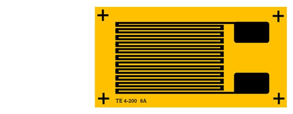
These devices incorporate a thin metallic foil grid bonded to a flexible backing. The grid’s serpentine pattern increases the length of the conductor in a compact area, enhancing sensitivity to strain in the required direction. The backing material provides mechanical support and electrical insulation for the foil grid. The adhesive layer bonds the backing and foil grid to the surface of the object being measured while the lead wires connect the strain gauge to external measurement devices such as a Wheatstone bridge circuit. While optional in controlled environments, a protective coating is often essential in outdoor or industrial settings to protect the sensor from moisture, chemicals and mechanical wear.
Applications
Foil strain gauges are widely used due to their affordability and ease of installation, making them widely adopted for structural testing and educational use.
- General structural testing: Suitable for measuring strain in beams, bridges, buildings and mechanical components. Foil gauges are cost-effective and easy to install on various surfaces.
- Educational and research facilities: Widely used in academic laboratories for teaching and early stage experiments due to their accessibility and ease of use.
- Short-term or non-critical monitoring: Effective for temporary load testing, prototype evaluation or systems where long-term durability is not essential.
- Large-scale sensor deployments: Their low cost enables widespread deployment across structures for distributed strain monitoring.
- Controlled environments: Perform reliably in indoor or stable conditions without requiring advanced environmental protection.
Considerations
Applications involving extreme temperatures, corrosive substances, or high pressure often lead engineers to reject foil strain gauges in favor of more robust alternatives.
Thin Film Strain Gauges
Thin film strain gauges are fabricated using microfabrication techniques that deposit a thin layer of metal or semiconductor material onto a substrate or – in some applications, directly onto the surface of the test specimen. Where electrical interference could affect performance, engineers may add an insulating layer between the substrate and the sensing layer. Similarly, a bonding layer such as titanium or chromium can improve adhesion between the sensing film and the substrate. Thin conductive traces or bonded wires connect the sensing element to external measurement circuits. As with foil gauges, a protective passivation layer is often applied to protect the gauge from environmental damage.
Applications
Thin film strain gauges are valued for their precision, stability, and ability to operate in harsh environments.
- Aerospace and automotive: Suited for high-temperature and high-stress environments due to their robust construction and minimal drift.
- Medical devices: Used in applications requiring miniaturization and biocompatibility, such as catheter-based sensors.
- MEMS devices: Integrated into microelectromechanical systems for compact and highly sensitive strain measurement.
- High-precision instrumentation: Suitable for laboratory-grade equipment where accuracy and repeatability are critical.
- Embedded monitoring: Can be directly deposited onto structural components for long-term embedded strain monitoring.
Considerations
Thin film strain gauges are often more expensive and complex to manufacture than foil gauges. In addition, these gauges require specific surface conditions or substrates for effective deposition of the sensing layer. Due to their limited flexibility, thin film gauges are not suitable for highly flexible or irregular surfaces.
Silicon Semiconductor Strain Gauges
Silicon semiconductor strain gauge technology uses the piezoresistive properties of doped silicon to measure strain. Unlike metallic gauges, these devices rely on changes in the crystal lattice structure of silicon under mechanical stress. These gauges feature a doped silicon element (typically p-type or n-type) whose resistivity changes in proportion to mechanical strain due to the piezoresistive effect. Often fabricated directly on a silicon wafer or bonded to a rigid carrier, in some designs the silicon itself acts as both sensing element and substrate. Engineers may use bonding agents or micromachining techniques to attach the gauge to the test surface. Metal contacts (e.g., aluminum or gold) deposited on silicon, connect the gauge to external circuitry. For sensors intended for demanding environments or where mechanical stress is expected, manufacturers offer a protective layer or housing to shield the gauge.
Applications
Known for their high sensitivity, engineers use silicon semiconductor strain gauges in precision and high-performance environments.
- Medical devices: Suited for miniature sensors in catheters, implants, and diagnostic equipment due to their small size and sensitivity.
- Aerospace and automotive: Used in environments requiring high accuracy and resistance to vibration and temperature extremes.
- Pressure sensors: Commonly integrated into MEMS-based pressure transducers and load cells.
- Industrial monitoring: Suitable for high-precision force and torque measurement in robotics and automation systems.
- Consumer electronics: Found in compact devices requiring integrated sensing capabilities.
Considerations
Engineers must use care when applying silicon semiconductor strain gauges since they are brittle and can fracture under excessive mechanical stress. These gauges are more expensive to manufacture than foil or thin film gauges and may require careful handling and encapsulation to provide reliability in harsh environments.
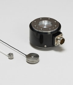
Microfused™ Technology
TE Connectivity's Microfused™ technology uses proprietary piezoresistive silicon elements fused directly to a metal diaphragm via high-temperature glass bonding. These sensing elements are integrated into strain gauge-based devices such as force sensors, pressure transducers, and load cells. This design creates a robust, monolithic sensing element with excellent long-term stability. The micromachined silicon piezoresistive element includes a Wheatstone bridge that directly converts mechanical strain to a voltage output signal, simplifying signal conditioning. These silicon sensing elements are permanently fused to a stainless-steel diaphragm with a high-temperature glass bonding layer which eliminates the need for adhesives or welds. Lead wires connect to silicon elements using proprietary wire bonding techniques, enabling reliable connections to signal conditioning electronics. This improves sensitivity, stability and durability in harsh environments. The entire assembly is housed in a rugged, sealed package designed to withstand extremely harsh environments and mechanical stress.
Applications
Devices that incorporate Microfused™ sensing elements are engineered for high-performance and high-volume environments where durability and precision are critical.
- Aerospace systems: Used in flight control sensors, flap jam detection, and autopilot force feedback systems.
- Medical devices: Suitable for compact, high-accuracy sensors in diagnostic and therapeutic equipment.
- Industrial automation: Suited for load cells, force sensors, and pressure transducers in demanding industrial settings.
- Automotive systems: Applied in braking, steering, and suspension systems requiring robust and reliable sensing.
- Test & measurement equipment: Integrated into precision instruments for dynamic force and pressure monitoring.
Considerations
Because of their unique features, MicrofusedTM strain gauges may require tailored packaging or electronics for specific applications. These gauges are more expensive than foil gauges due to advanced materials and manufacturing processes. Integration of MicrofusedTM sensors may require careful design considerations for optimizing performance in embedded systems.
Comparison Chart
| Category | Feature | Microfused Silicon | Foil | Semiconductor (Silicon) | Thin Film |
|---|---|---|---|---|---|
| Performance | Signal Output | Very high | Low | High | Moderate |
| Signal Stability | Excellent | Moderate to Poor | Very Good to Excellent (with proper packaging) | Exceptional | |
| Sensitivity (Gauge Factor) | 50 - 200 | 1 - 5 | 50 - 200 | ~2 | |
| Response Time | Fast | Moderate | Very Fast | Fast | |
| Reliability | Hysteresis | Very Low | Moderate to High | Very Low | Low |
| Creep Resistance | Exceptional | Poor | Excellent | Excellent | |
| Fatigue Life | Very Long | Shorter | Very Long | Long | |
| Environmental Tolerance | Temperature Range | Up to 750°F | Up to 350°F | Up to 750°F | High (application dependent) |
| Durability | Exceptional (glass-bonded, fatigue-resistant) | Moderate (organic backing, adhesive creep) | Excellent (rigid crystalline structure) | Excellent (molecularly bonded, fatigue resistant) | |
| Leak Potential | Leak-proof (hermetic seal) | High risk (adhesive degradation) | Moderate (mounting dependent) | Low risk (substrate dependent) | |
| Noise Immunity | High | Low | High | Moderate | |
| Cost Efficiency | Size | Compact | Larger | Micro-machinable | Ultra-thin |
| Integration | Monolithic (glass-bonded) | Surface-mounted (adhesive) | Substrate-compatible (package dependent) | Substrate-integrated (deposited) | |
| Cost | Moderate | Low | Moderate to High | High |
Microfused Advantage
When integrated into strain gauge-based devices, TE Connectivity’s MicrofusedTM silicon sensing elements offer several key advantages when integrating into strain gauge-based devices, making them a superior choice for high-performance applications. Their unique construction -- fusing piezoelectric silicon directly to a metal diaphragm using high-temperature glass bonding -- ensures exceptional long-term stability and durability. This design eliminates the need for adhesives or welds, reducing potential failure points and enhancing reliability. Incorporating a micro-Wheatstone bridge into each sensor simplifies signal processing and TE’s proprietary wire bonding techniques improve their sensitivity and stability.
These features, when incorporated into a rugged, sealed package ensure that MicrofusedTM devices can withstand extreme conditions, making them suitable for aerospace, medical, industrial, automotive and test and measurement applications. Overall, TE’s MicrofusedTM silicon technology enables robust, reliable and high-performance strain sensing solutions for precise strain measurement in a wide range of critical applications.