Enabling a Safer, Greener, and Connected World
By continuously developing materials and processes to print electronic components, TE’s Printed Electronics team is enabling customers to build transformative technology.
Authors:
Yiliang Wu, Principal Scientist, Material Development
Gokce Gulsoy, Senior Scientist, Material Development
Leonard Radzilowski, Staff Scientist, Material Development
The Advantage of Printed Electronics. Printed electronics technology aims to create electronic devices using a set of printing methods to deposit functional materials into a patterned structure on various substrates, in a similar manner to how newspapers are printed on paper. It provides an eco-friendly, agile, and flexible way to cost-effectively drive innovation and manufacturing. In contrast to conventional newspaper printing, functional materials with desired electrical properties and advanced printing processes with enhanced resolution and accuracy are critical. Within TE’s Printed Electronics team, based in Freemont, California, our scientists are developing novel material formulations and printing technologies for three application areas: contact finishes for harsh environment connectivity, antennas for wireless connectivity, and sensors for smart connectivity.
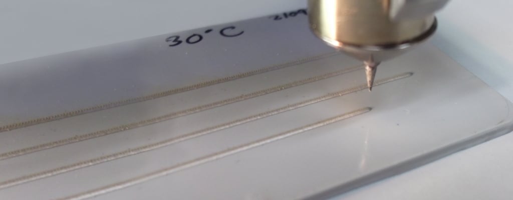
Electrically conducting inks patterned directly onto dielectric substrates using various printing processes can...increase the available range of permittivity compared to typical printed circuit board (PCB) substrates...
The first focus area is to utilize conductive ink printing technology to fabricate contact finishes for harsh environment electrical connectors. The process can be successfully scaled up to roll-to-roll production by applying the conductive ink on a flexible feedstock using a gravure printer, drying the volatile contents of the ink, and finally stamping/forming the feedstock to the finished connector form. For low level signal and voltage applications, the process can offer significant (up to 70%) cost savings by increasing the process speed (e.g., up to 30m/min), eliminating wet chemistry/deposition and replacing gold with cheaper technically viable contact finish alternatives which may not be fabricated using the conventional electroplating process. For power transmission and connector applications, the process enables faster production speed – which yields substantial cost savings. This sustainable, “dry-floor” process can also help eliminate cyanide baths and reduce fire hazards, waste generation, and energy/water consumption. This technology is enabling our Printed Electronics team to launch new materials and products, attract new customers in every industry we serve, and differentiate TE as an innovation leader.
Another area that printed electronics can impact is antenna manufacturing. At TE, we work closely with customers to design and manufacture antennas for different types of applications – for example, in aircraft, hand-held consumer devices, or automobile infotainment and safety – with very different requirements. One trend that is consistent across all applications is the need to reduce antenna size, weight, power consumption, and cost. Electrically conducting inks patterned directly onto dielectric substrates using various printing processes can help realize these goals. Non-conventional substrates, for example, increase the available range of permittivity compared to typical printed circuit board (PCB) substrates, which facilitates smaller antenna sizes with comparable bandwidth as well as reduced power consumption and cost. Importantly, printed conductive inks can metallize these novel materials where MID methods such as laser direct sintering (LDS) and two-shot molding cannot. In our laboratory, our Printed Electronics team has successfully printed on a variety of plastics and plastic composites, glass, and ceramics. We have demonstrated our ability to print over 3D shapes using digitally-driven robotic printers. This ability may lead to novel, 3D space-filling antennas that better optimize antenna size, efficiency, and bandwidth by utilizing a greater amount of the available package volume. The digital process additionally facilitates design changes without the expense and delay of creating new tooling. As antenna applications continue to grow, we look forward to further developing TE’s printed metallization capabilities to deliver metallized surfaces with complex shape, robust durability, and low cycle time.
The last focus area is to apply printed electronics technology in sensors, which is one of TE’s core business sectors. The global sensors market is growing, driven by rising demand for a smarter, interconnected world, as exemplified by the internet-of- things ecosystem. For customers in automotive, industrial, medical devices, and consumer electronics, this technology helps improve performance, reduce cost, and achieve desired form factors. In our laboratory, we devote our efforts to applying printed electronics technology to address these challenges by using novel materials and simplified fabrication process. We have explored the printing of nanoparticle silver inks as electrodes for ultrasonic image sensor applications. Small particle size leads to a significant reduction of surface roughness of screen printed electrodes, and, as a result, a substantial improvement of image quality. Miniaturized magnetic structures could find applications in position, speed, liquid level, and torque sensors. Such tiny magnetic structures, which could not be made using a conventional molding process, can be directly printed using magnetic inks onto either a flat or a curved surface, not only reducing the size but also simplifying the integration process. As sensors have a very diversified market with a high potential for customization, we envision that printing technology will provide advantages for sensor fabrication, especially for low-volume and high-mix devices.
Solutions Helping Customers
TE’s Printed Electronics team is continuously developing materials and processes to print electronic components for connectivity applications. Specially, we are increasingly exploring new ink technologies, such as conductive inks, magnetic inks, and other functional inks. And we are using different kinds of printing technologies –gravure, stencil/screen, dispense jet printing – to fabricate functional devices, including metal contacts, antennas, and sensors. By focusing on innovation, we can help our customers build the things that make the world safer, sustainable, productive, and connected.